
DNX–SENS–NV02
CHF 9’900 per unit
• Four independently controlled sensing zones
• Independent microwave and RF control
• Pulsed-measurement capability
Back to shop
Multi-zone precision sensing at atomic scale
The DNX–SENS–NV02 Four-Quadrant NV-Diamond Quantum Sensor is designed for laboratory, industrial and advanced-research teams requiring spatially resolved magnetic-field, temperature and materials measurements without cryogenic infrastructure. A 10 mm × 10 mm NV-diamond sensing plate is combined with four independently addressable sensing zones, enabling simultaneous, sequential or comparative measurements across multiple locations on the same diamond.
Each zone incorporates Dynex’s proprietary nested-loop excitation architecture, with dedicated microwave and RF structures for electronic- and nuclear-spin control. The compact loop geometry replaces a conventional large ring resonator, producing localized excitation fields while preserving independent control of the four measurement zones.
The platform supports multi-point magnetic-field mapping, thermal-gradient measurements, materials characterisation, current-distribution analysis and advanced pulsed-ODMR workflows. Its modular RF architecture is designed for integration with external microwave sources, pulse generators, RFSoC systems, lock-in amplifiers and optical acquisition hardware.
Parameters
Parameter | Specification |
|---|---|
Sensor type | Four-quadrant NV-Diamond Quantum Sensor |
Sensing platform | Solid-state nitrogen-vacancy diamond |
Diamond size | 10 mm × 10 mm |
Independently addressable zones | 4 |
Operating principle | Optically detected magnetic resonance |
Operating environment | Room temperature |
Measurement capabilities | Magnetic-field, temperature and materials characterisation |
Zone arrangement | Four sensing regions distributed across one diamond plate |
Local excitation hotspot | Approximately 1.5 mm × 1.5 mm per zone |
Microwave control | Independent microwave loop for each zone |
RF control | Independent RF loop for each zone |
Total excitation channels | 8 |
Microwave inputs | 4 independently addressable 50 Ω ports |
RF inputs | 4 independently addressable 50 Ω ports |
Supported measurement modes | Continuous-wave, modulated and pulsed ODMR |
Optical readout | Zone-selective NV photoluminescence detection |
Proprietary Excitation Architecture
Parameter | Specification |
|---|---|
Architecture | Nested microwave and RF current-loop structure |
Microwave-loop position | Inner loop |
Microwave-loop dimensions | 2.6 mm × 2.6 mm |
RF-loop position | Outer loop surrounding microwave loop |
RF-loop dimensions | 3.5 mm × 3.5 mm |
Feed architecture | 50 Ω transmission line |
Simulated input impedance | Approximately 47 Ω |
Return path | Via-connected bottom ground plane |
Microwave design range | 2.0–4.0 GHz simulated |
Primary NV operating frequency | Approximately 2.87 GHz |
RF operating range evaluated | 100 kHz–20 MHz |
Substrate | Transparent quartz glass |
Substrate thickness | 0.5 mm |
Quartz dielectric constant | Approximately 3.8 |
Quartz optical transmission | Greater than 90% |
The inner microwave loop provides localised excitation near the NV zero-field-splitting frequency, while the surrounding RF loop supports lower-frequency spin-control and experimental protocols. Both structures use dedicated feed lines and ground returns, providing independent control of every zone.
The transparent quartz substrate supports optical access through the sensing assembly while providing suitable dielectric properties for both microwave and RF structures.
Simulated Excitation Performance
Parameter | Specification |
|---|---|
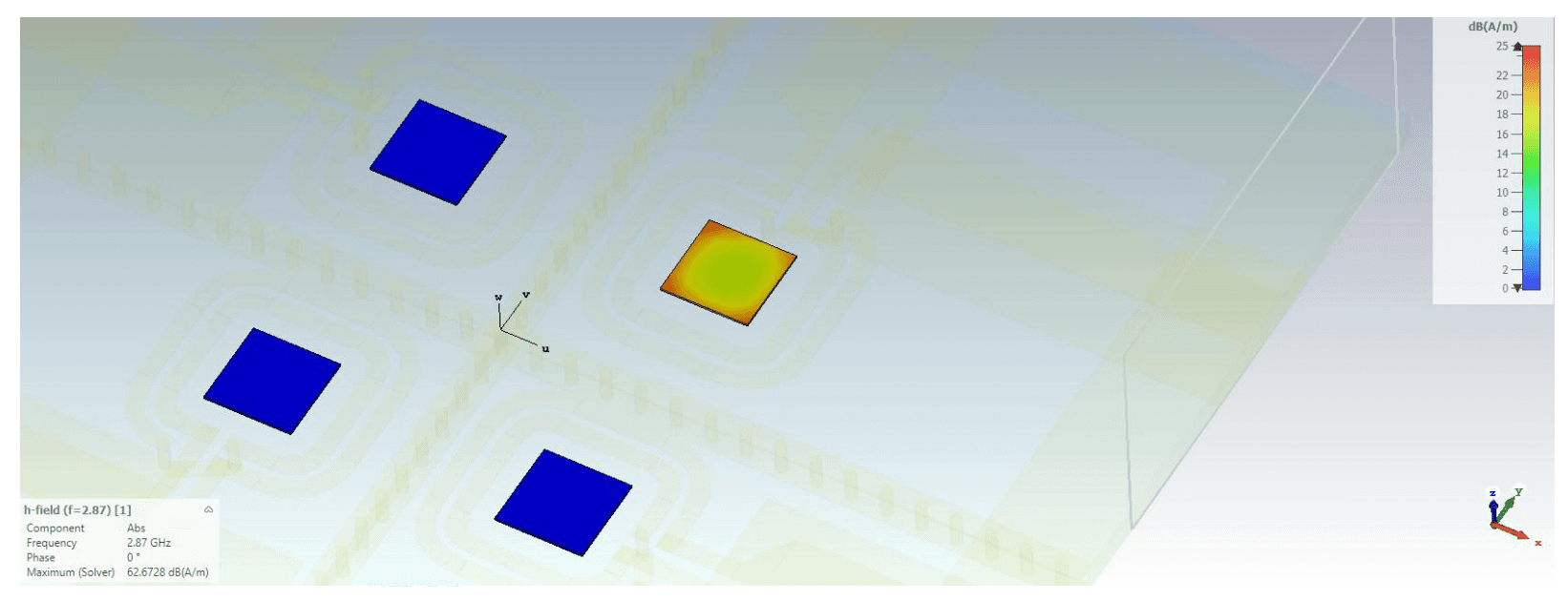
Microwave field-map frequency | 2.87 GHz |
Microwave excitation power used in simulation | 1 W per active port |
Minimum microwave field in modeled hotspot | Approximately 16.5 A/m |
Equivalent microwave B₁ field | Approximately 0.2 G |
Typical microwave isolation between zones | 30–35 dB |
Lowest simulated adjacent-zone isolation | Approximately 20 dB |
RF excitation power used in simulation | 1 W per active port |
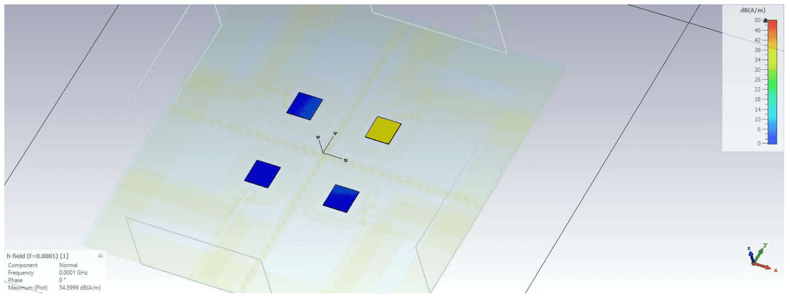
Simulated RF magnetic field | Approximately 36.5 A/m |
Equivalent RF B₁ field | Approximately 0.46 G |
RF frequency response | Broadband across 100 kHz–20 MHz |
The microwave simulations show localized excitation of the selected zone at 2.87 GHz, with the remaining zones receiving substantially reduced field intensity. Typical simulated isolation between microwave channels is approximately 30–35 dB.
The RF-loop structure remains comparatively constant across the evaluated 100 kHz to 20 MHz range, supporting broadband control rather than operation at only one narrow resonant frequency.
NV-Diamond Characterisation
Parameter | Specification |
|---|---|
Diamond format | 10 mm × 10 mm NV-diamond plate |
Optical characterization | Photoluminescence spectrum |
Spin-resonance characterization | Continuous-wave ODMR |
Coherence characterization | Hahn-echo measurement |
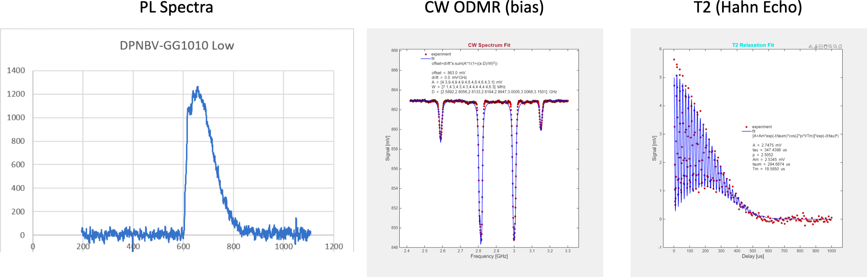
Measured Hahn-echo coherence time | Approximately 350 µs |
ODMR response | Multiple resolved resonance features |
Supported workflows | CW ODMR, bias-field measurements and pulsed spin experiments |
The diamond characterization includes photoluminescence spectroscopy, continuous-wave ODMR under bias field and Hahn-echo coherence measurements:
Integrated Optical Detection
Parameter | Specification |
|---|---|
Detector material | Silicon |
Detector architecture | Reverse-biased PIN photodiode with fixed-gain transimpedance amplifier |
Active area | Ø 1.0 mm / 0.8 mm² |
Wavelength range | 200–1100 nm |
Peak response wavelength | 730 nm, typical |
Peak responsivity | 0.44 A/W, typical |
Small-signal bandwidth | 150 MHz |
Rise time | 2.3 ns |
Noise-equivalent power | 2.92 × 10⁻¹¹ W/√Hz |
Output noise | 1.5 mV RMS |
Maximum dark offset | ±10 mV |
Maximum output current | 100 mA |
Supported load impedance | 50 Ω to high-impedance |
Transimpedance gain at 50 Ω | 5 × 10³ V/A, ±2% |
Transimpedance gain at high impedance | 1 × 10⁴ V/A, ±2% |
Output voltage at 50 Ω | 0–5 V |
Output voltage at high impedance | 0–10 V |
Detector-stage supply | +12 VDC / ground / −12 VDC |
Detector operating temperature | 10–40 °C |
Detector storage temperature | −20–70 °C |
The integrated optical detectors support visible and near-infrared fluorescence monitoring over a 200–1100 nm wavelength range. Their buffered outputs can drive either 50 Ω or high-impedance acquisition inputs, with output ranges of 0–5 V and 0–10 V respectively.
Key Features
Four independently controlled sensing zones
The four-quadrant architecture enables comparative measurements, spatial-gradient sensing and localized excitation without mechanically repositioning the diamond.
Room-temperature quantum sensing
NV centers retain optically readable spin properties at room temperature, removing the need for cryogenic cooling infrastructure.
Independent microwave and RF control
Each sensing zone has a dedicated microwave loop and a dedicated RF loop, providing eight individually addressable excitation channels.
Localized microwave excitation
The compact inner-loop geometry concentrates the microwave field within the intended sensing region while reducing excitation of neighbouring zones.
Broadband RF capability
The surrounding RF loops support control signals from approximately 100 kHz to 20 MHz, enabling nuclear-spin manipulation, low-frequency excitation and advanced pulse sequences.
Transparent quartz architecture
The quartz-glass substrate permits optical access to the NV diamond while supporting microwave and RF routing beneath the sensing surface.
Multi-point measurement workflows
Four sensing regions can be used to compare local magnetic fields, temperature gradients or material responses within one synchronized experimental platform.
Pulsed-measurement capability
The combination of microwave control, broadband RF excitation and demonstrated Hahn-echo coherence supports advanced spin-manipulation and coherence-based sensing protocols.
Applications
Multi-point magnetic-field measurement
Magnetic-field-gradient mapping
Current-density and conductor diagnostics
Temperature and thermal-gradient sensing
Advanced materials characterization
Semiconductor and electronic-device diagnostics
Battery and energy-storage research
Biomedical and surface-field measurements
Pulsed ODMR and spin-coherence experiments
Quantum-sensing research and instrumentation